|
|
 |
 |
| AJIT Processor IP Core |
| To enlarge the picture please click on it. |
|
|
|
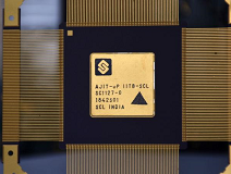
AJIT Processor IP Core
Instruction set: IEEE std. 1754-1994 (SPARC V8) RISC instruction set. 64-bit/32-bit/16-bit/8-bit load/store instructions. 64-bit/32-bit IEEE 754 floating point arithmetic: including divide and square-root.
32K I/D caches (virtually indexed, virtually tagged), Memory-management-unit (MMU).
Micro-architecture: In-order 5-stage instruction execution pipeline (1 instruction per clock cycle). 8 register windows, pipelined load/store unit, pipelined floating point unit (single precision and double precision). Branch predictor and speculative execution of predicted instruction stream, mispredict penalty: 4-20 cycles. All exceptions handled precisely (including floating point exceptions), interrupts checked at every instruction.
Hardware debug monitor (4 hardware break/watch points), GDB remote debug capabilities.
|
- Interfaces: AHB lite system bus
- Operating modes: Normal pipelined mode: pipeline runs normally, at full speed. Debug mode: processor connects to remote debugger and breakpoint/watch-point monitoring enabled in the pipeline. Single-step mode: processor operates in single-step mode, pipelining is disabled. Logger mode: processor produces log of stores and register writes in the pipeline.
- Processor platform components: Processor models: C ISA model, C microarchitecture model, synthesizable VHDL. Software: linux 3.16.1 port, GCC compiler, GDB debugger.
- Silicon Proven
|
|
Top
|
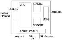
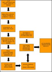
| Verification Methodology with IMAGE Simulation Acceleration |
| To enlarge the picture please click on it. |
|
|
|
Simulation Accelerator; IMAGE 2.0 [1x4]
Are your Simulations taking long time?
IMAGE solves this; it accelerates your simulation and that too at an unbelievable low price.
IMAGE (aka I Made A Great Emulator) is the flagship product. It is the best price-performance affordable simulation accelerator in the world. IMAGE 2.0 is a world-class engineered, simulation accelerator for functional verification with a performance of 100X during the iterative debug-compile-run phase and 1000X during the regression phase of the design cycle. It is particularly suited for large designs. It is the best price-performance verification tool for complex designs for all applications, be it processors, telecom, memory, multimedia, automobile etc.
|
|
FPGA based Simulation Accelerator
IMAGE 2.0 is based on an array of FPGAs. It has a scalable architecture that supports from 5 to 100 million gate capacity, delivering from 100X to 1000X acceleration over pure simulation for [Verilog, VHDL, mixed] language designs.
By virtue of the price-performance parameter, IMAGE 2.0 is today the Worlds best simulation accelerator.
Features
- The best price-performance affordable simulation accelerator in the world.
- Inbuilt parallelism for fast Synthesis.
- Mixed-language, VHDL and Verilog compatible.
- Acceleration: 100X to 1000X compared to gate-level simulation; around 100X speed improvement, compared to RTL simulation.
- Plug-and-Play Simulation-like Flow; replacing the call to the simulator of choice with a call to IMAGE 2.0 and uses any standard synthesis tool.
- Scalable Capacity: From 5 Million to 456 Million gates.
- Memory capacity from 24 to 380 MB.
- Design Controllability.
- Design Observability.
- Multi-clock & true asynchronous clock behaviors.
- Memory extraction for optimization.
- Support for Black-Box & user defined unsynthesizable module.
- Onsite support for IMAGE as well as for Verification.
|
| Top |
|
|
|
 |
|
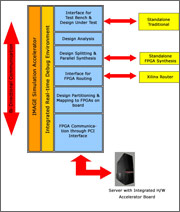
Design Methodology with IMAGE-MultiCloX
|
|
To enlarge the picture please click on it.
|
|
IMAGE-MultiCloX
If one was trying to build an FPGA prototype of an ASIC?
OR
If one was trying to implement RTL on an FPGA?
One would hit the limitation on the number of clocks to be implemented on the FPGA. IMAGE-MultiCloX solves this limitation.
IMAGE-MultiCloX is a Second generation tool of IMAGE family. MultiCloX helps resolve the limitation
on number of "clocks implemented on an FPGA device".
|
|
IMAGE-MultiCloX takes a synthesizable design and produces a functionally equivalent synthesizable design which can be targeted to any FPGA device.
|
-
Deploying MultiCloX in the design flow, the original RTL with multiple clocks would be transformed to a functionally equivalent RTL with a single clock for FPGA device mapping.
-
MultiCloX would also transform the original design, to automatically map memories in the RTL design to embedded memories (e.g. Block RAMs) on the FPGA device.
-
Additionally an access bus would be provided along with the transformed design, to observe and control user-specified internal signals in the original design.
|
| Top |
|
|
|
 |
|
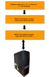
IMAGE Reconfigure System
|
|
To enlarge the picture please click on it.
|
|
IMAGE Reconfigure System
Currently FFT, Vector Multiplication etc and languages like C, C++, FORTRAN etc are being used on IMAGE Reconfigure System.
IMAGE Reconfigurable computing Lab is a computing paradigm combining some of the flexibility of software with the high performance of hardware by processing with very flexible high speed computing fabrics like FPGAs. The principal difference when compared to using ordinary processors is the ability to make substantial changes to the data path itself in addition to the control flow.
|
|
IMAGE Reconfigure System
IMAGE Reconfigure System offers a number of features that make it ideally suited for Reconfigurable Computing.
IMAGE Reconfigure System comes with a FPGA Capacity from 20 Million FPGA Gates to 100 Million FPGA Gates; with multiple processors and huge memory bank.
The logic of an FPGA is determined by a configuration, similar to software, so that an FPGA can be reconfigured to perform a variety of computations without redesigning the hardware. An FPGA blurs the distinction between hardware and software. The "hardware" fabricated by a foundry is general purpose; consequently they are mass produced and affordable. The logic of an FPGA is also customized by loading a "configuration," which is similar to a software program. High-level configuration languages (in particular, VHDL and Verilog) support FPGA configuration design, and commercial tools like partition of the design (PartIT from Powai Labs), memory extraction (MiRAGE from Powai Labs), forcing a signal to “0” or “1” (ForceIT from Powai Labs), signal visibility tool (HookIN from Powai Labs), simulation and synthesis tools; and processors that compliment the FPGAs i.e. a hybrid of FPGAs and processors.
Some of our customers use IMAGE Reconfigure System for unprecedented computing power.
|
| Top |
 |
|
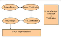
System Design, Validation & Verification
|
|
To enlarge the picture please click on it.
|
|
System Design, Validation & Verification
In today's high technology business, cost efficiency and faster time to market is a challenge that all organizations are facing. More so in the VLSI and system design arena where reliability, quality and first time right solutions are of paramount importance because of very high costs of iterations. With expertise of some of the best global talent
|
|
in-house, we can assist you with your product development goals.
|
|
For Verification & Validation, we have experts along with the best-in-class proprietary tool IMAGE for regression testing, deep simulation etc; we study your architecture, design and the process; we come-up with Verification plan, test bench etc; we can also map the final SoC on a proprietary FPGA Board etc.
We understand your needs and work either along with your teams at your site or take complete responsibility of delivering guaranteed functional success.
|
| Top |
|
|
For more details, please drop us an email at:
us@powailabs.com
-----------------------------------------------------------------------------
Copyright © Powai Labs Technology Pvt. Ltd.
All Rights Reserved.
Copyright law and international treaties protect the content of this page. Any reproduction or distribution of this document or any portion of this website, in any form by any means, without the prior written consent of Powai Labs Technology Pvt. Ltd. is prohibited. All company, brand and product names are trade or service marks, or registered trade or service marks, of Powai Labs Technology Pvt. Ltd. or of their respective owners.
|
|
 |
|
IMAGE System
|
|
To enlarge the picture please click on it.
|
|
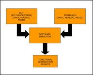 |
| Stand-Alone Simulator Verification flow |
|
To enlarge the picture please click on it.
|
|
 |
|
IMAGE Simulation Accelerator Verification Flow
|
|
To enlarge the picture please click on it.
|
|
 |
|
IMAGE FPGA Board
|
|
To enlarge the picture please click on it.
|
|
|